
 Yahoo Finance
 Onto Innovation Debuts Sub-surface Defect Inspection for Advanced Packaging
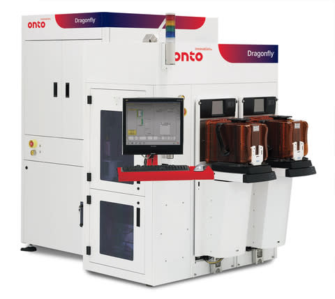

New capability released for the Dragonfly® G3 inspection system enables 100% wafer inspection for critical sub-surface defects
Onto has received multiple orders in support of high bandwidth memory (HBM), advanced logic and a variety of specialty segments
WILMINGTON, Mass., April 23, 2024--(BUSINESS WIRE)--Onto Innovation Inc. (NYSE: ONTO) today announced the release of a new sub-surface inspection capability for the Dragonfly® G3 sub-micron 2D/3D inspection and metrology platform. The new capability enables whole wafer inspection for critical yield impacting defects that can lead to lost die as well as entire wafers breaking in subsequent process steps. Such defects were previously impossible to find in a production environment. In today’s world of wafer thinning and multi-layer wafer or die bonding, sub-surface defects are far more dangerous than ever before as bonded layers are now a tenth of their former thickness and far more brittle and therefore more susceptible to damage pre- or post-bonding. Sub-surface defects that occur during the bonding or thinning process such as micro-cracks can cause not only die yield issues, but wafers can be shattered resulting in the loss of hundreds of die in an instant.
Now, Onto Innovation is offering the capability to detect these yield killing defects on the well-established Dragonfly platform at production speeds. By using novel infra-red (IR) technology and specially designed algorithms, the Dragonfly platform provides customers a choice to scan the entire wafer for hidden defects rather than be limited to sampling only selected areas of the wafer. This greatly impacts final yield and cost savings through reduced scrapped wafer/die stacks.
"Customers are demanding 100% inspection capability with production-worthy throughput," says Mayson Brooks, vice president and general manager of Onto’s inspection business. "The Dragonfly G3 system’s new high speed IR capability delivers just that, combined with the flexibility to select from multiple objective lenses allowing customers to inspect at different magnifications for different applications and devices."
"The Dragonfly G3 system with its enhanced sub-surface defect detection builds upon the previous model’s successful adoption by HBM customers for die position metrology on stacked dies and wafers," says Brooks.
According to TechInsights, the market for inspection products supporting wafer level packaging (WLP) is forecast to grow from $400 million in 2024 to more than $600 million by 2028. The advanced node portion of this market supporting new HBM technologies as well as advanced GPUs used in artificial intelligence (AI) applications is currently outgrowing the overall market with an annual growth rate of >19%.
For more information about the high speed IR capability on the Dragonfly G3 system, contact us or reach out to your local sales team.
About Onto Innovation Inc.
Onto Innovation is a leader in process control, combining global scale with an expanded portfolio of leading-edge technologies that include: Un-patterned wafer quality; 3D metrology spanning chip features from nanometer scale transistors to large die interconnects; macro defect inspection of wafers and packages; metal interconnect composition; factory analytics; and lithography for advanced semiconductor packaging. Our breadth of offerings across the entire semiconductor value chain combined with our connected thinking approach results in a unique perspective to help solve our customers’ most difficult yield, device performance, quality, and reliability issues. Onto Innovation strives to optimize customers’ critical path of progress by making them smarter, faster and more efficient. With headquarters and manufacturing in the U.S., Onto Innovation supports customers with a worldwide sales and service organization. Additional information can be found at www.ontoinnovation.com.
Forward Looking Statements
This press release contains forward-looking statements within the meaning of the Private Securities Litigation Reform Act of 1995 (the "Act") which include statements relating to Onto Innovation’s business momentum and future growth; the benefit to customers and the capabilities of Onto Innovation’s products and customer service; Onto Innovation’s ability to both deliver products and services consistent with our customers’ demands and expectations and strengthen its market position, Onto Innovation’s beliefs about market opportunities as well as other matters that are not purely historical data. Onto Innovation wishes to take advantage of the "safe harbor" provided for by the Act and cautions that actual results may differ materially from those projected as a result of various factors, including risks and uncertainties, many of which are beyond Onto Innovation’s control. Such factors include, but are not limited to, the Company’s ability to leverage its resources to improve its position in its core markets; its ability to weather difficult economic environments; its ability to open new market opportunities and target high-margin markets; the strength/weakness of the back-end and/or front-end semiconductor market segments; fluctuations in customer capital spending; the Company’s ability to effectively manage its supply chain and adequately source components from suppliers to meet customer demand; the effects of political, economic, legal, and regulatory changes or conflicts on the Company's global operations; its ability to adequately protect its intellectual property rights and maintain data security; the effects of natural disasters or public health emergencies, such as the COVID-19 pandemic, on the global economy and on the Company’s customers, suppliers, employees, and business; its ability to effectively maneuver global trade issues and changes in trade and export regulations and license policies; the Company’s ability to maintain relationships with its customers and manage appropriate levels of inventory to meet customer demands; and the Company’s ability to successfully integrate acquired businesses and technologies. Additional information and considerations regarding the risks faced by Onto Innovation are available in Onto Innovation’s Form 10-K report for the year ended December 30, 2023, and other filings with the Securities and Exchange Commission. As the forward-looking statements are based on Onto Innovation’s current expectations, the Company cannot guarantee any related future results, levels of activity, performance or achievements. Onto Innovation does not assume any obligation to update the forward-looking information contained in this press release, except as required by law.
Source: Onto Innovation Inc.
ONTO-IP
View source version on businesswire.com: https://www.businesswire.com/news/home/20240423254870/en/
Contacts
Investor Relations:
Michael Sheaffer, +1 978.253.6273
mike.sheaffer@ontoInnovation.com
