
 Yahoo Finance
 Archer Materials advances to wafer-scale quantum device fabrication

Image 1
Highlights
12CQ chip development advances to wafer-scale quantum electronic device fabrication using foundry-compatible UV optical and E-beam lithography.
Hundreds of quantum electronic devices and qubit materials prepared for testing, measurement, integration, and optimisation towards qubit control and readout.
Archer engaging with tier-one semiconductor companies, including TSMC to secure future manufacturing capabilities, and service and support technology development.
The Company is well capitalised with approximately A$24.3 million cash and no debt.
SYDNEY, Australia, April 05, 2023 (GLOBE NEWSWIRE) -- Archer Materials Limited (“Archer”, the “Company”, “ASX: AXE”) is pleased to provide shareholders an update on the progress of its 12CQ chip development. During the past months the Company’s progress has involved the following:
Development of a multi-scale wafer fabrication process for Archer’s quantum electronic devices.
Commencing technical programs of low-temperature (cryogenic) characterisation of quantum electronic devices necessary for the development of qubit readout and control mechanisms in Archer’s chip-based quantum logic devices.
Advances in optimising and validating the 12CQ qubit material coherence times.
Development of an encapsulation method for the 12CQ qubit chips. Initial outcomes of the packaging development indicate cleanroom processing is compatible with standard semiconductor foundry methods while maintaining coherence times.
Collaboration with researchers at EPFL, and since late 2022, the Company and EPFL have been developing second-generation, unique integrated chip designs for the potential complex spin manipulation of Archer’s qubit material.
TSMC (the largest semiconductor foundry in the world) has accepted Archer as their customer after due diligence and screening. This permits Archer to access TSMC semiconductor fabrication process technologies, which include the most advanced technologies and also more mature process technologies.
Commenting on Archer’s 12CQ chip development progress, Company CEO Dr Mohammad Choucair said: “Archer is making considerable progress across several fronts in 12CQ technology development. The Company’s technical achievements are providing a strong basis for pursuing external engagement with tier-one semiconductor companies.
“Archer Materials is now a company firmly on its growth path. Our focus remains very sharply on quantum work and related semiconductor operations and we continue to advance methodically towards our goals.”
Wafer-scale quantum electronic device fabrication
Archer staff, working at a Sydney-based prototyping semiconductor foundry have recently developed a multi-scale wafer fabrication process for its quantum electronic devices. Wafer-based functional devices (“chips”) are a fundamental requirement to the development of the 12CQ chip technology, as Archer’s innovation aims to realise mobile-compatible quantum processing that can easily be integrated into modern electronic devices.
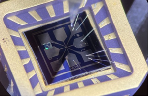
The Company devised and applied methods that combine both UV optical lithography and electron-beam (E-beam) lithography, two of the most common semiconductor nanofabrication techniques, to facilitate the fabrication of potentially hundreds of advanced quantum electronic devices (“QEDs”) on a single silicon wafer (Image 1). This has greatly increased the yield of QEDs that are being developed and optimised to address Archer’s technological goals of quantum control and readout in the 12CQ chip-based qubit system.
Advanced quantum measurements, equipment, facilities, and infrastructure
Archer continues to address the sector scarcity of available and accessible world-class facilities to perform the sophisticated quantum measurements required for 12CQ chip development. Archer has now secured access to a local state-of-the-art cryogenic quantum device measurement laboratory and commenced technical programs of low-temperature (cryogenic) characterisation of QEDs. While the Company’s technology remains focused on quantum devices that can operate at room-temperature, the cryogenic measurements are necessary to advance development of qubit readout and control mechanisms in Archer’s chip-based quantum logic devices.
Integration of Archer’s unique quantum material into chip-based functional devices is key to the Company’s 12CQ Project. Archer has recently advanced its methods for patterning nanometre-scale qubit material into QEDs. These QEDs integrating qubit material have allowed for ongoing testing and measurements that aim to validate quantum electronic properties that could potentially be exploited towards qubit readout approaches (Image 2). The improved device designs include an increased number of electronic leads as well as gate electrodes to control the electronic states within the devices.
Since late 2022, the Archer team has been establishing the Company’s own, customised laboratory facility, with the core of the facility now operational and located at the Sydney Hardware Lab (Image 3). The laboratory is equipped with basic and advanced R&D tools, plant, and equipment for the dedicated, efficient processing of quantum materials, and includes specialty instruments assembled by Archer for the electronic characterisation of its QEDs.
The Company has made advances in optimising and validating the 12CQ qubit material coherence times. Recently, the Archer team prepared, and characterised the coherence properties of over 150 separately synthesised qubit material batches. These materials will be used in the integration with hundreds of QEDs planned for on-chip measurements and testing throughout 2023. The resulting information will be used for characterising the performance of the qubit and evaluating its suitability for specific quantum technology and computing applications.

Image 1. An Archer 4 x 4 mm single-chip quantum electronic device after installing and bonding into a commercial chip carrier. This completed device is compatible with measurement setups for electronic characterisation at cryogenic temperatures as well as ambient conditions at room temperature using Archer’s in-house lab capabilities as well as external facilities.
Semiconductor fabrication and chip architecture engineering
There is an operational and process requirement for a vacuum or inert atmosphere environment when operating the 12CQ qubit material to preserve coherence times. The development by Archer of the use of an inert atmosphere was a significant advance over the use of vacuums. Further still, the packaging of future 12CQ devices in a semiconductor foundry requires significant innovation in materials and process engineering to maintain qubit properties (e.g. coherence), operation, and function.
Archer is working towards a potential breakthrough in the foundry packaging of the 12CQ chip architecture. Archer’s nanodevice engineers are developing an encapsulation method for the 12CQ qubit chips, that could potentially provide an ‘artificial vacuum’ to allow devices to be operated in ambient conditions. Initial outcomes of the packaging development indicate cleanroom processing is compatible with standard semiconductor foundry methods while maintaining coherence times. This means the approach has the potential for technology translation to industrially scale Archer’s 12CQ qubit chip architecture.
Collaboration with EPFL
Archer continues to collaborate with researchers at EPFL. Since late 2022, the Company and EPFL have been developing second-generation, unique integrated chip designs for the potential complex spin manipulation of Archer’s qubit material. The new chip designs significantly advance on the HEMT and CMOS chip designs and functionality reported in 2022. The new chips are being manufactured in a semiconductor foundry in Europe, with ongoing testing, optimisation, and potential operation anticipated throughout 2023.
In November 2022, the Company reported that powerful supercomputer simulations provided the most accurate understanding of Archer’s unique 12CQ qubit material to date, confirming a metallic-like nanocarbon. Since then, the detailed scientific results of the work have been collated and submitted for publication in a scientific journal. The submission is undergoing the routine peer-review process, with publication expected in the second half of 2023.
Engagement with global semiconductor supply chain participants
TSMC has accepted Archer as their customer after due diligence and screening. This permits Archer to access TSMC semiconductor fabrication process technologies, which include the most advanced technologies and also more mature process technologies (e.g. 180 nm and 130 nm processes). This will allow Archer to perform cost-effective multi-project wafer runs, and potential tape out and industrial production of future devices. Contractual relationships with TSMC will be on a case by case basis. TSMC is the largest semiconductor foundry in the world.
About Archer’s 12CQ chip technology
Archer’s 12CQ chip innovation aims to develop a carbon-based spin qubit and integrate this quantum technology with modern semiconductor devices. Recent progress towards this goal has involved fabricating wafer-scale quantum electronic devices, completing advanced quantum measurements, advances in chip architecture engineering, second-generation integrated quantum device development, and engagement with tier-one semiconductor companies.
About Archer
Archer is a technology company that operates within the semiconductor industry. The Company is developing advanced semiconductor devices, including chips relevant to quantum computing and medical diagnostics.
The Board of Archer authorised this announcement to be given to ASX. | For more information about Archer’s activities, please visit our: |
|
|
A photo accompanying this announcement is available at https://www.globenewswire.com/NewsRoom/AttachmentNg/c5ab5ded-13d9-4061-ae94-c963ce673d41

